Quantitative strain mapping at the nanometer scale (Vol. 43 No. 1)
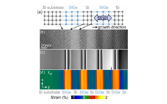
 (a) Scheme and (b) dark-field (004) electron hologram of a Si/Si0.79Ge0.21 superlattice. (c) Phase of the hologram. (d) Strain map.
As strain is now used routinely in transistor devices to increase the mobility of the charge carriers, the microelectronics industry needs ways to map the strain with nanometer resolution. Recently, a powerful TEM (transmission electron microscopy) based technique called dark-field electron holography has been invented by Martin Hÿtch at CEMES in Toulouse. To map the strain, it is necessary to thin a sample to electron transparency using a focused ion beam tool. Then, to form a dark-field electron hologram, electron beams that have been diffracted by both the region of interest (a device, a layer) and a region of reference (usually the substrate) are interfered using an electron biprism.
When grown on a Si substrate by epitaxy, SiGe layers are tensily strained in the growth direction as shown in Figure (a). Due to the presence of strain, variations of the hologram fringe spacing can be seen (b). Using Fourier space processing, the phase of the electrons can be retrieved from the hologram (c), and by taking the gradient of the phase, the strain map can then be calculated (d).
As the technique is quantitative, one can directly correlate the results with simulations to get information about the composition in the layers. As an example, we have investigated the variation of the substitutional carbon content in annealed Si/SiGeC superlattices. Carbon is used to control the strain and avoid plastic relaxation. However during annealing, the formation of Β-SiC clusters reduces the effect of the C atoms. By combining holography and finite element simulation, we have shown that after annealing at 1050°C, a SiGeC structure behaves like pure SiGe from the point of view of strain.
The reduction of the substitutional C content in annealed Si/SiGeC superlattices studied by dark-field electron holography
T. Denneulin, J. L. Rouvière, A. Béché, M. Py, J. P. Barnes, N. Rochat, J. M. Hartmann and D. Cooper, Semicond. Sci. Technol. 26, 125010 (2011)
[Abstract]


